
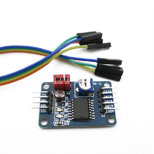
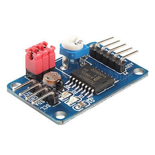
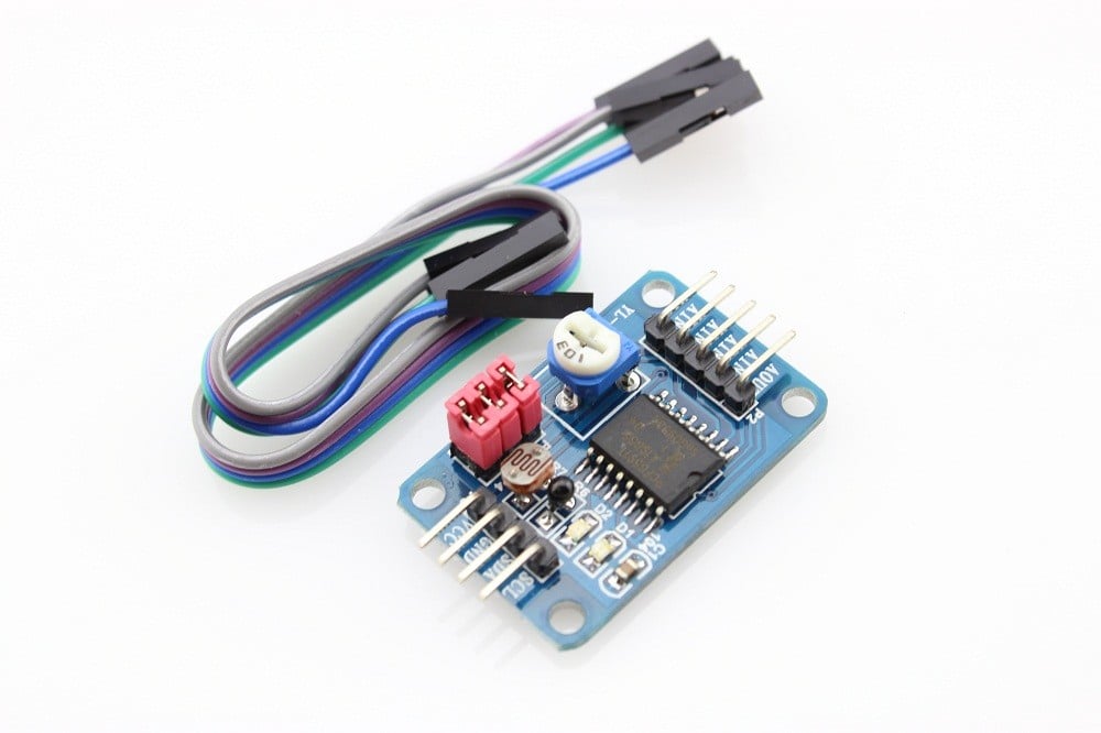
PCF8591 Module Analog to Digital / Digital-Analog Converter Module with F-F Jumper Wire
₹176
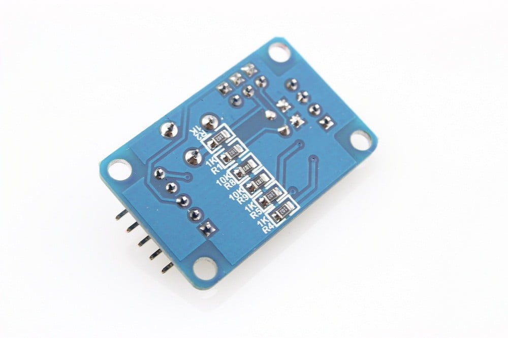
Module chip using PCF8951
Module supports external voltage input of the 4-way acquisition (voltage input range of 0-5v)
The module integrated photoresistor by AD collection precise value of the ambient light intensity
Module integrated thermistor by the precise value of the ambient temperature of the AD acquisition
Module integrated 1 channel 0-5V voltage input acquisition (the blue potentiometer to adjust the input voltage)
Modules with power indicator (for the module power supply indicator lights)
Modules with DA output indicator, when the module DA output interface voltage reaches a certain value, will be lit panel the DA output indicator, the higher the voltage, the more obvious indicator brightness
Out of stock
Description
This is a breakout board/Prototype Board for PCF8591 IC. The PCF8591 Module Analog to Digital / Digital-Analog Converter Module with F-F Jumper Wire is a single-chip, single?supply low?power 8?bit CMOS data acquisition device with four analog inputs, one analog output, and a serial I?C?bus interface. Three address pins A0, A1, and A2 are used for programming the hardware address, allowing the use of up to eight devices connected to the I?C?bus without additional hardware. Address, control, and data to and from the device are transferred serially via the two-line bidirectional I?C?bus.
The functions of the device include analog input multiplexing, on-chip track and hold function, 8-bit analog?to?digital conversion, and an 8?bit digital?to?analog conversion. The maximum conversion rate is given by the maximum speed of the I?C-bus.
PCF8591 IC Features
Single power supply
A PCF8591 operating voltage range of 2.5V-6V
Low standby current
Via I2C bus serial input/output
PCF8591 by 3 hardware address pins addressing
PCF8591 I2C bus speed sampling rate decided
4 analog inputs programmable single-ended or differential input
Automatic incremental channel selection
PCF8591 analog voltage range from VSS to VDD
PCF8591 built-in track-and-hold circuit
8-bit successive approximation A / D converter
1 analog output DAC gain
Module Features
The module supports external voltage input of the 4-way acquisition (voltage input range of 0-5v)
The module integrated photoresistor by AD collection precise value of the ambient light intensity
Module integrated thermistor by the precise value of the ambient temperature of the AD acquisition
Module integrated 1 channel 0-5V voltage input acquisition (the blue potentiometer to adjust the input voltage)
Modules with power indicator (for the module power supply indicator lights)
Modules with DA output indicator, when the module DA output interface voltage reaches a certain value, will be lit panel the DA output indicator, the higher the voltage, the more obvious indicator brightness
Module PCB size: 3.6cm x 2.3cm
A standard double panel, thickness 1.6mm, nice layout, surrounded by a through-hole, aperture: 3mm, convenient fixed.
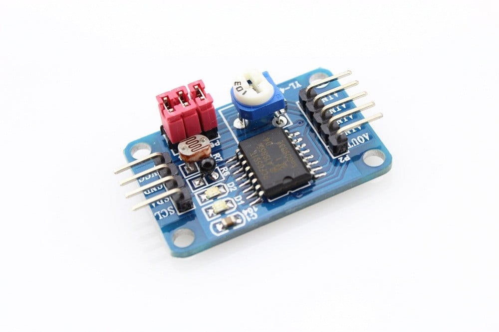
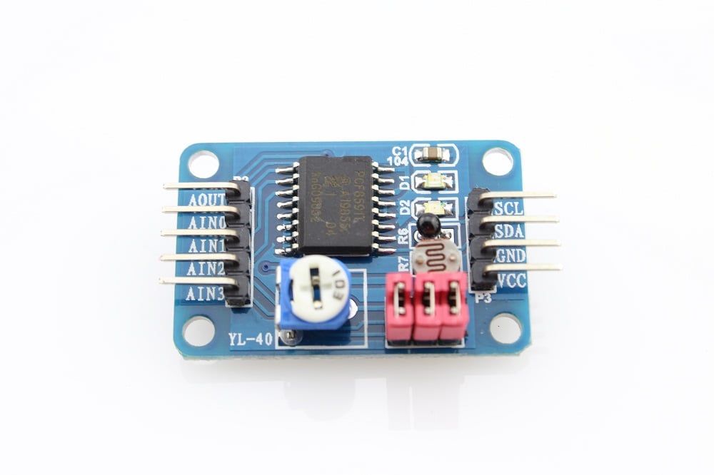
Module interface specification
The Left
AOUT chip DA output interface
AINO chip analog input interface 0
AIN1 chip analog input interface 1
AIN2 chip analog input interface 2
AIN3 chip analog input interface 3
The Right
SCL ? IIC clock interface connected to microcontroller IO port
SDA ? IIC digital interface connected to microcontroller IO port
GND ? connected to ground
VCC ? connected to 3.3v-5v
Four red jumper-cap instruction
P4 ? connected to P4 shorting cap, select thermistor access circuit
P5 ? connect P5 shorting cap, select photoresistor access circuit
P6 ? connected to P6 shorting cap, select 0-5V adjustable voltage access circuit
Package?Includes:
1 x?PCF8591 Module Analog to Digital / Digital-Analog converter module with F-F Jumper Wire
Additional information
| Weight | 0.06 kg |
|---|---|
| Dimensions | 8 × 7 × 3 cm |
Only logged in customers who have purchased this product may leave a review.
Reviews
There are no reviews yet.